高解像度画質によるお客様の固有のニーズに合わせたイメージングソリューション
Jenoptikは、お客様の市場での成功をさらに強化できるよう支援し、皆様のアプリケーションにぴったり適したイメージングコンセプトとソリューションを提示します。

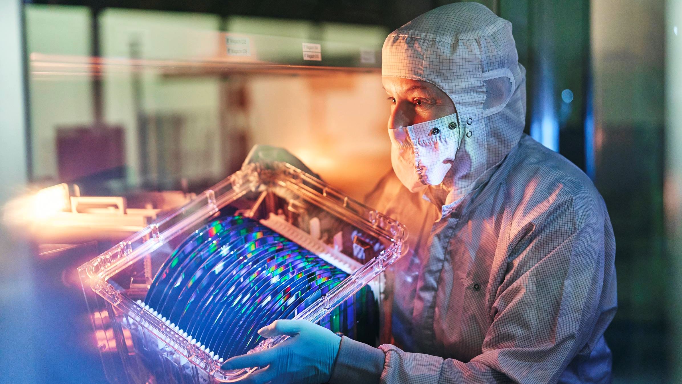
私たちの高機能カメラ、画像処理製品および完全なOEMシステムは、科学・産業用イメージング市場での理想的なソリューションです:私たちは量産プロジェクトおよび個別プロジェクトの両方に対応する画像モジュールを供給します。
私たちはお客様のご要望すべてに正確に適合する製品をご提供しています。 — さらに完全なバリューチェーンをご提供しています: センサーとセンサーボードからお客様固有のアプリケーション向けの自社ファームウエアを備えたカメラシステム・ソリューションまで対応しています。
私たちは、お客様のニーズにあわせて、コンパクトなCMOS USBカメラモジュールのベーシックバージョンを最適化します。5メガピクセルの解像度およびUSB 2.0インターフェースを持つこのモジュールは理想的なプラットフォームをご提供します。お客様に固有のカスタム変更に、非常に短納期で対応いたします。さらに、私たちは、マイナーチェンジを行ったハードウエアやソフトウエア、あるいはお客様の画像処理アプリケーションにあわせ、異なるモジュールから完全なシステムを構築することもできます。
より複雑なプロジェクトでは、お客様のご要望にあわせて、私たちのカメラモジュールの性能および機能を組み合わせることができます。
こうしたカスタマイズは次のものを含んでいます:
さらに、私たちは専門のサブライチェーンマネジメントの提供によりお客様を支援し、お客様の全バリューチェーンを管理します。私たちは、全工程の明瞭な概観を維持し、お客様の製品の市場への投入を迅速に進め、持続可能な成功を支援します。
私たちはお客様のご要望すべてに正確に適合する製品をご提供しています。 — さらに完全なバリューチェーンをご提供しています: センサーとセンサーボードからお客様固有のアプリケーション向けの自社ファームウエアを備えたカメラシステム・ソリューションまで対応しています。
私たちは、お客様のニーズにあわせて、コンパクトなCMOS USBカメラモジュールのベーシックバージョンを最適化します。5メガピクセルの解像度およびUSB 2.0インターフェースを持つこのモジュールは理想的なプラットフォームをご提供します。お客様に固有のカスタム変更に、非常に短納期で対応いたします。さらに、私たちは、マイナーチェンジを行ったハードウエアやソフトウエア、あるいはお客様の画像処理アプリケーションにあわせ、異なるモジュールから完全なシステムを構築することもできます。
より複雑なプロジェクトでは、お客様のご要望にあわせて、私たちのカメラモジュールの性能および機能を組み合わせることができます。
こうしたカスタマイズは次のものを含んでいます:
- 波形率。
- 解像度 (1 MP, 3 MP, 5 MP, 10 MP, 14 MP, ...).
- センサー・タイプ (CCD / CMOS)。
- デジタル・インターフェース(USB 2.0, USB 3.0)。
- 光学インターフェース (C-マウント, S-マウント, CS-マウント)。
- 光学製品、フィルター、その他。
画像システムの成功を実現する専門知識
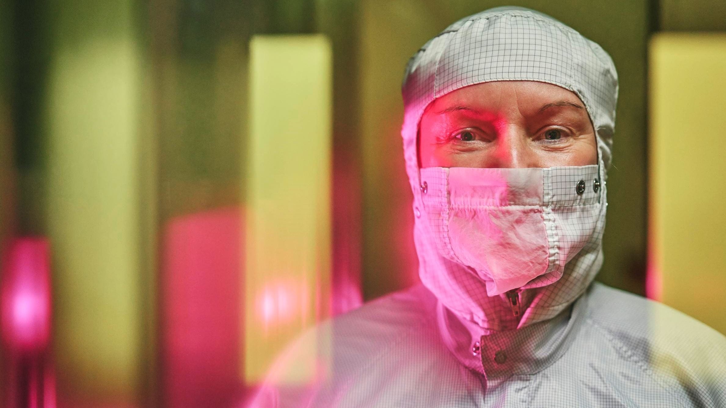
私たちは、お客様の成功を支援する画像システムをご提供します。Jenoptikのエキスパートが、皆様のプロジェクトの全体にわたって皆様を支援し、かつシステム・パートナーとして皆様と緊密に協業します:私たちは設計過程を管理し、実現可能性の検討を行ない、さらにOEMカメラ設計を担当します。これによって、プロトタイプを製作し、できるだけ短い時間でお客様のイメージング・ソリューションを市場に投入することを可能にします。さらに、私たちは専門のサブライチェーンマネジメントの提供によりお客様を支援し、お客様の全バリューチェーンを管理します。私たちは、全工程の明瞭な概観を維持し、お客様の製品の市場への投入を迅速に進め、持続可能な成功を支援します。
Our Expertise
- 17 years of know-how in the production of opto-electronic systems
- Unique selling point: Inline LED module measurement technology
- Rapid Protoyping
- Design for Manufacturing
- Well-founded advice on product development, qualification and series transition
ISO Certificates
- DIN EN ISO 9001 (QM-System)
- DIN EN ISO 13485 (Medical Application)
- ISO 14001 (Environment Management System)
Department Production Information
- Department exists since 2006 at Jenoptik
- Area: approx. 400m²
Area consists of two clean room classes:
- 2/3 of the area ISO class 5 (max. 832 particles with 1 µm/m³)
- 1/3 of the surface ISO class 7 (max. 83,200 particles with 1 µm/m³)
Process steps in detail
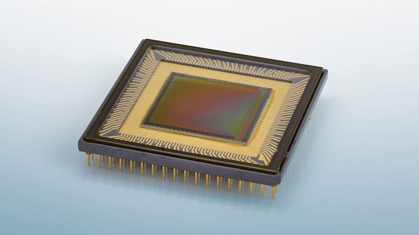
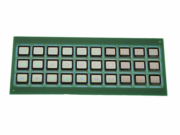
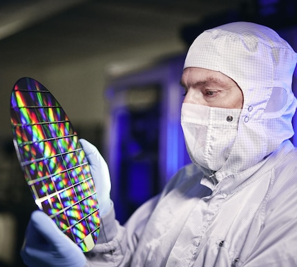
An Imagesensor as example
Learn more about our core competencies for customer imaging modules
Dicing
Die-Bonding
Wire-Bonding
Housing
Testing
Separation
Core competence Dicing

Semiconductor Wafer
Substrate sizes
- Diameter up to 12 inches
- Thickness 0.1mm to 5mm
- Accuracy: up to 2 µm
Creation of negative 3D structures
- Increase adhesive surface for later bonding
- Change reflection characteristics
Full underwater separation option with following benefits
- Increase purity
- ESD safety through conductance controlled ultrapure water
Separable Materials
- Ceramics and sintered ceramics
- PCB materials / metals
- Composite materials and plastics
- Silicon / glass
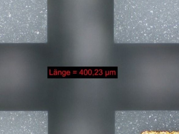
Application Examples for Dicing
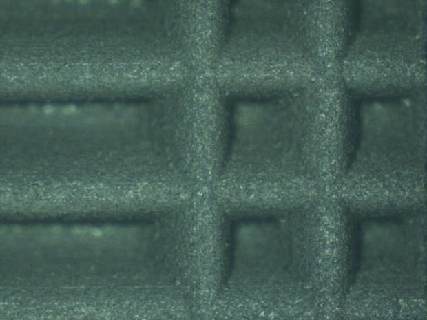
3D structure to increase adhesive surface (180µm)
Cut in sintered ceramics
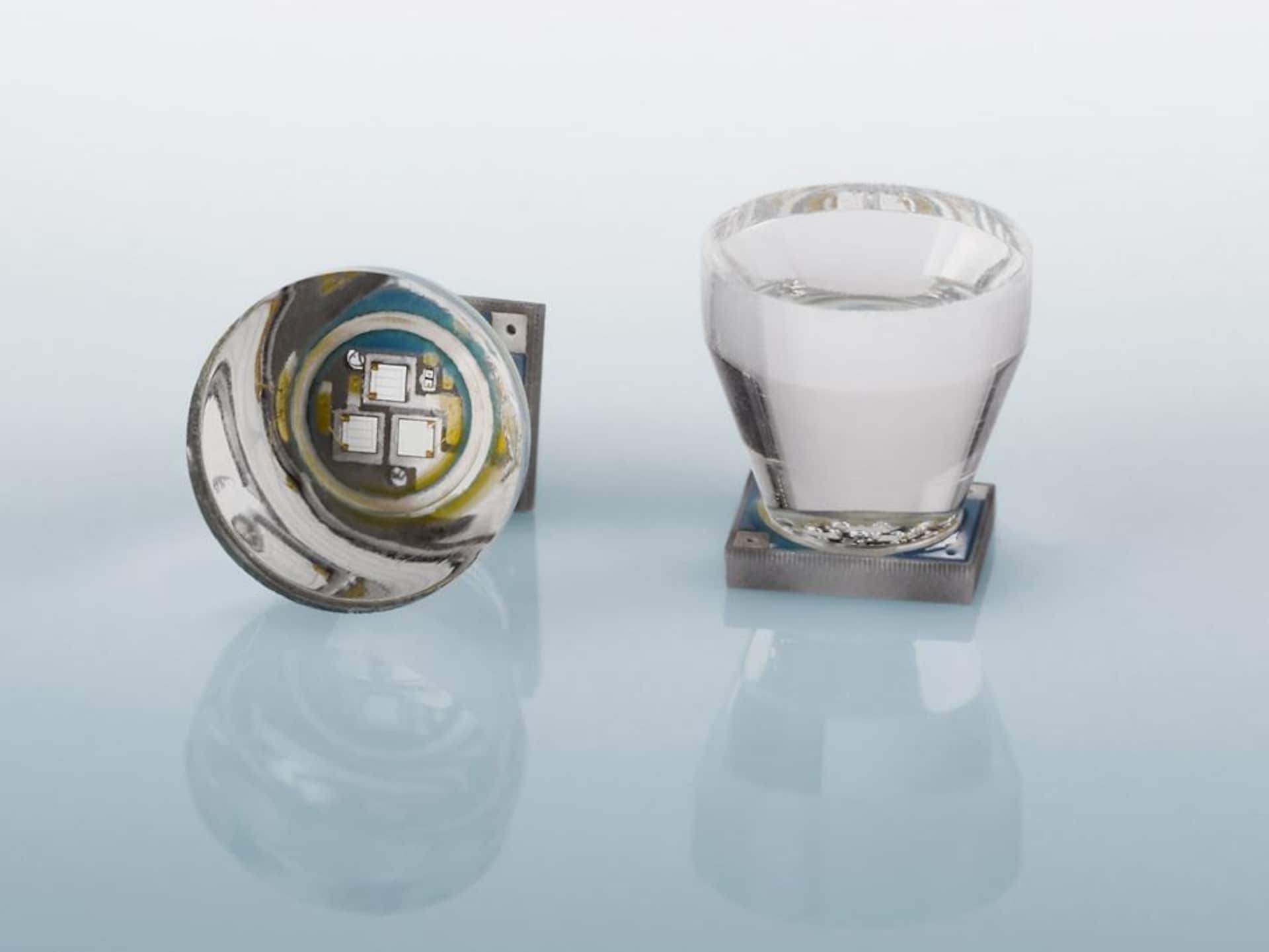
Core competencies Die-Bonding
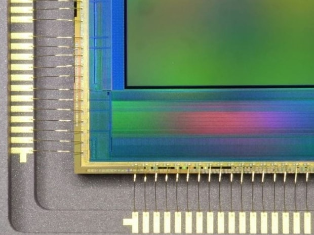
Full Format Image Sensor (Au, Ball-Wedge, 25µm)
Technology
- Adhesive die bonding (inline dispensing & stamping)
- Sintering
- Stacked die bonding
- Flip chip technology
Applications
- Wafer-level packaging (WLP) of MEMS and sensors
- Flip chip
- LED modules
- Image sensors
- Handling of image sensor with micro lens arrys
Substrates
- Circuit boards, wafers, component carriers, lead frames
Component dimensions
- 0.17mm up to 50mm
- > 25µm thickness
- Accuracy up to < 5µm
Component feed options:
- Wafer, waffle / Gel-Pak, reel
Marking
Technology
- Laser marking
- Printing system (Ink Jet)
Applications
- Traceability
Cleaning
Technology
- barrel reactor
Applications
- Clean organic residues from surface
- Activate surface (increase adhesion forces during joining processes)
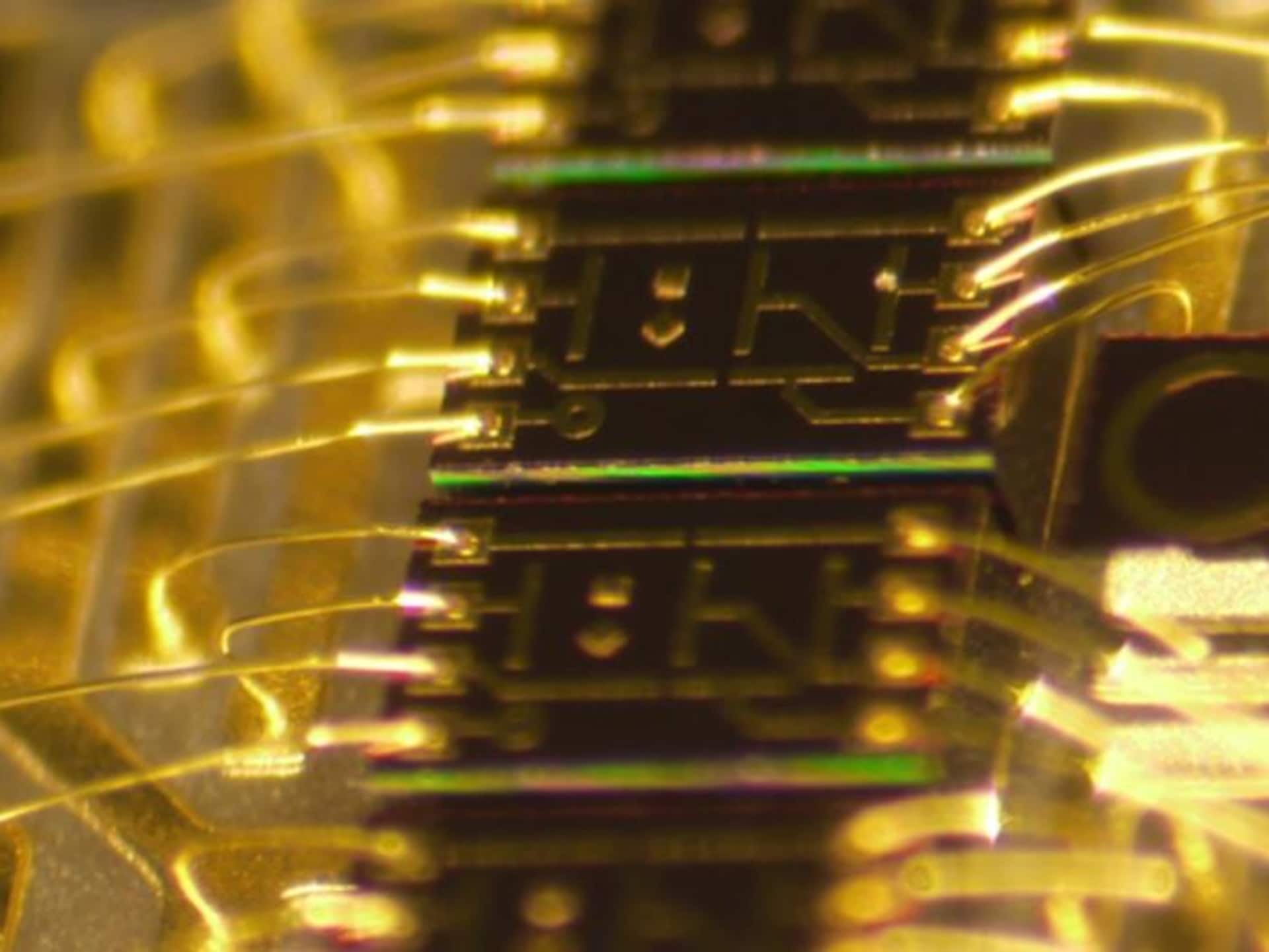
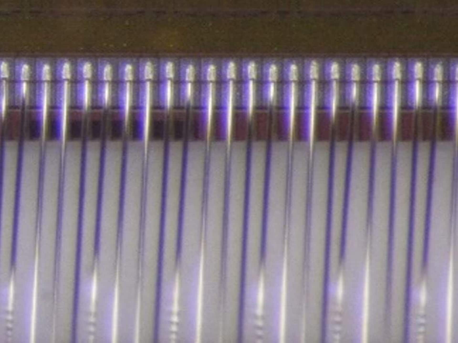
Core Competence Wire-bonding
Technology
- Wedge-Wedge and Ball-Wedge
- Accuracy bond tool: 2.5 µm
- Wire diameter: 12.5 µm up to 75 µm
- Material: gold, aluminum, silver, copper, and platinum
Core competence
- Adjust loop profile for ultra flat bonds
- Reflection-poor ball-wedge technology
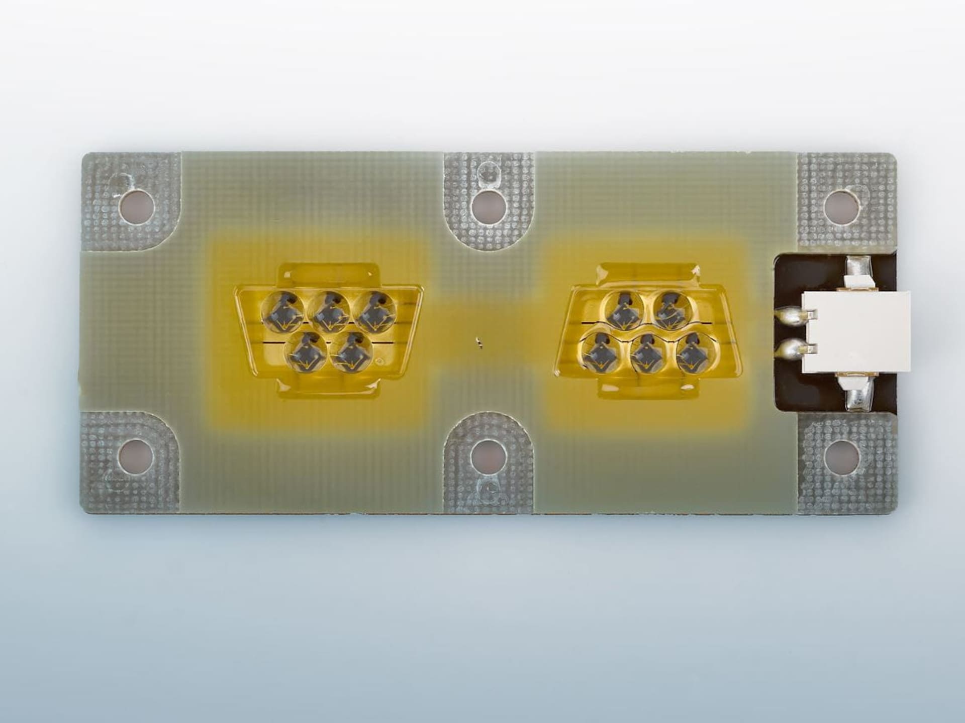
Core competence Housing: Dispensing
Technology
- Accuracy 14µm
- Volume- or mass-controlled dispensing
- Volume accuracy: 0.1µl
Materials
- Silicone (in different cleanroom)
- 2/3K epoxy, polyurethane
Special competences
- Dam fill / underfill
- Black encapsulation to reduce reflections
- Mechanical protection
- Optical encapsulation to change light parameter
Core competence Housing: Set and seal optics
- Accuracy (regarding die-bonding) < 5µm
- Processing of special epoxy resins
- Minimization of trapped air (special evacuation procedure)
- Cavity flushing with N2 during the setting process
- Curing of potting with temperature or UV light
Core competence: EOL-Test
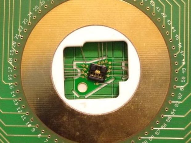
Opto-electrical measurement and AOI, contacting with card according to customer design
Probing-Station
- Accuracy up to 3µm
- Current-voltage characteristics
- 40W Current/voltage source with 4-point measurement
- Radiant intensity and wavelength measurement
- Automatic optical inspection (AOI)
- Applicatio12 MP Camera
- Switching/multiplexing with up to 32 contacts
- Logic measurements, multi-segment displays, etc.
- Flying probe
Further Product Recommendations

ご不明な点はございませんか?私たちのエキスパートが喜んでご回答いたします。


Digital Imaging & Optoelectronic Systems
HCI-CN-Carl-Wang
EditContact
Sales Jenoptik Japan
+81 045 670-9141
Sales North America