RecommendMail Facebook LinkedIn
UFO Probe® カード - PIC ウエハー試験用の新テストカード
フォトニック集積回路(PIC)は、未来のチップです。インテグレートされたフォトニクスは、電気の代わりに光を使用して、データと信号の処理を行います。
The needs of chip manufacturers
- Increased chip complexity and integration density (SoC) through monolithic or heterogeneous integration of optics and electronics
- Economies of scale for cost optimization
- High-throughput test solutions for high-volume production
- High-yield mass production to reduce scrap and losses
- Automated test solutions
- Standardized tests
Challenges in Silicon Photonics Testing
- High-throughput test solutions (suitable for fab requirements) that perform electronic-photonics testing at the wafer level, with high parallelism and as much automation as possible
- Functional testing of PICs at an early stage in the process is critical for higher yields
- Standardization of the test environment and procedures is necessary to enable consistent and predictable testing of silicon photonics.
Free webinar recording: Watch it now and learn more!

“Just the Right PIC – How Advanced Test Concepts Enable Fast PIC Wafer-Level Testing!”
In this exclusive webinar recording, Tobias Gnausch (Jenoptik) and Sylwester Latkowski (TU Eindhoven) provide valuable insights into the following topics:
- Characterization vs. Testing: What are the differences, and why are both indispensable?
- Standardization as a foundation: How uniform test standards form the basis for high-volume production.
- Optoelectronic test methods: Practical approaches that allow you to significantly increase the efficiency of your wafer production
- Reliable testing without “active alignment”: Innovative techniques that eliminate the need for time-consuming alignments while guaranteeing the highest measurement accuracy.
世界をスピードアップ
Custom-designed for a variety of applications
Unlike traditional test solutions, which use separate optical and electrical probe cards, Jenoptik combines an electrical and an optical test module into a single, compact test card. This test card is custom-designed and combines Jenoptik’s expertise in optics and photonics with the established probe technology of leading manufacturers.
Depending on your requirements, the UFO Probe® Card is configured and manufactured to meet your specific needs. Here are three examples of ProbeCard configurations we have already implemented. Contact us to discuss your individual requirements.

UFO Probe® Cantilever in Eurocard Format
- For vertically emitting PICs
- Monolithically integrated optical module with standardized or custom inputs and outputs
- Cantilever probe technology with several hundred probes
- Standard probe interface: Eurocard format
- Integrated distance sensor.

UFO Probe® Vertical in Eurocard format
General operating principle similar to that of the UFO Probe Cantilever, but particularly suitable for…
- High probe counts of up to tens of thousands of probes and beyond
- Extremely small probe sizes and spacings down to >40 µm
- Testing of pads and bumps
- Suitable for multi-DUT (multi-chip) and high-frequency (HF) testing.

UFO Probe® Vertical in ATE format
- Direct-docking design
- Interface for system integration into ATE (automated test equipment) platforms, such as Advantest V93000 or Teradyne UltraFlex
- For vertical-emitting PICs
- Ideal for a high number of electrical and optical contacts, as well as for multi-DUT testing.
Customized for your success
Each UFO Probe® Card is customized to the individual requirements and the respective wafer layout and is available with both cantilever and vertical needle technology. Check out the specifications for more details.

All benefits of the Probe Card Technology on one view
進歩
PIC エコシステムは、高スループット連続生産向けの効率的な検査方法によって拡張できます。また、複数のチップの並列検査通過により検査時間を短縮できます。
革新性
標準の検査装置で使用できる大量生産向けの唯一の商用検査ソリューション。
品質
スクラップは生産の初期段階で特定され、歩留まりの改善につながります。すべての PIC の全検査は、ウェハー上で実施されます。
プラグ&プレイ
標準的な IC テスターと自動テスターで作動するように設計されています。低い出費と試運転費用。
効率的
故障部品が早期に発見されることで、歩留まりの向上と生産フローの最適化が可能です。
柔軟性
光学式 I/O チャンネルのピッチと数は、お客様に合わせて設定できます。
現在および将来のプローブカードの用途


UFO Probe® カードで IC と PIC の並行検査が可能です
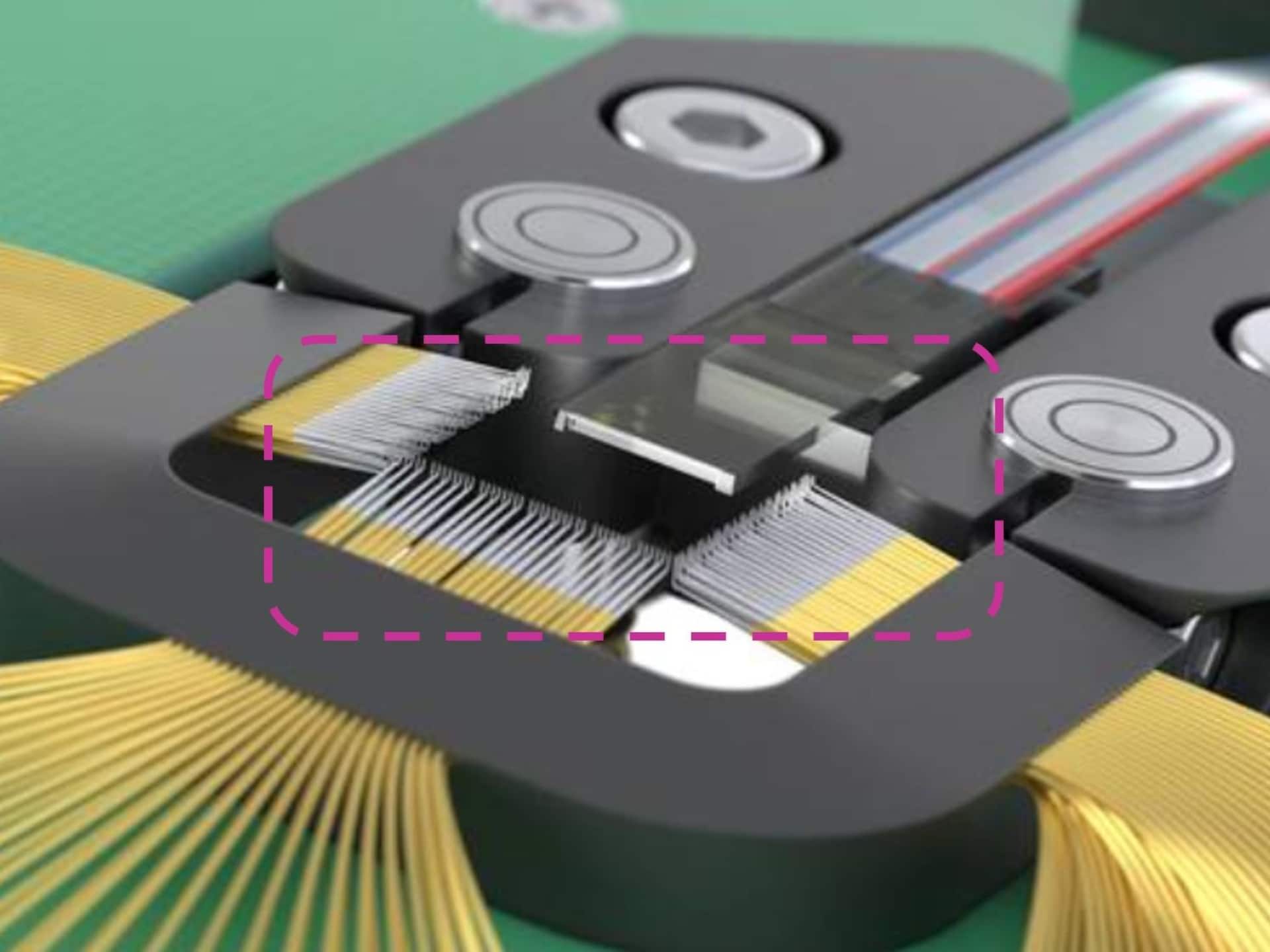
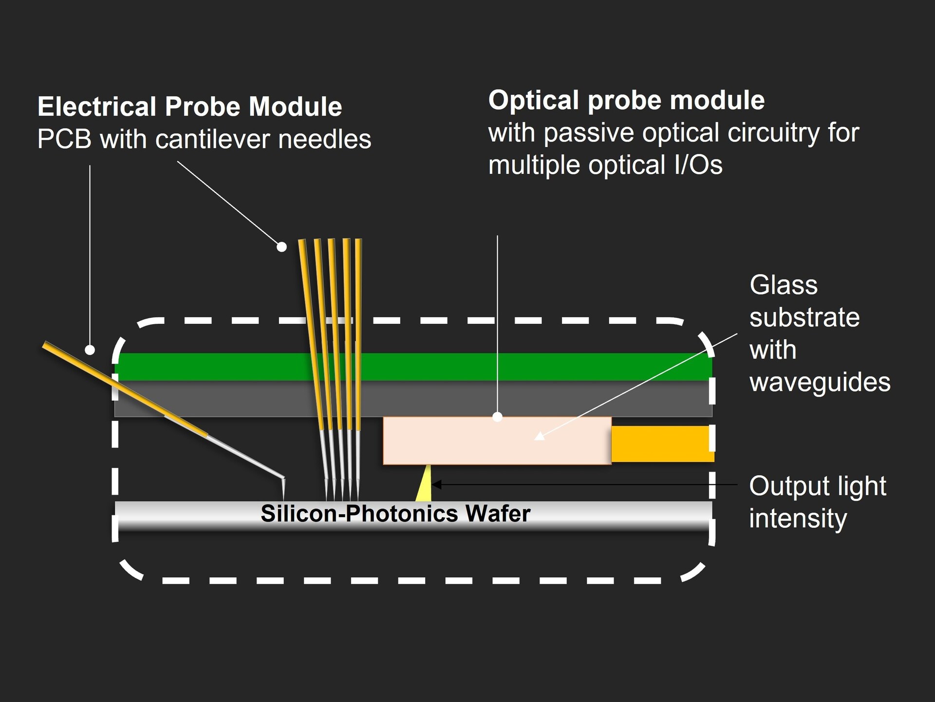
- Monolithically integrated optical module
- Alignment-insensitive optical coupling for vertically emitting PICs (compensates for probe tolerances)
- Simultaneous bonding of the chip’s optical and electrical interfaces
- Use of field-proven probe technologies
- Standard interfaces to testers and wafer probers
UFO Probe® オプトエレクトロニクスカードの技術的詳細
仕様 | 現世代 | 未来の世代 |
検査されるコンポーネント | 電子およびフォトニック集積回路(EPIC)、データ伝送および電気通信用の光トランシーバー | トランシーバー、フォトダイオード、 |
電気ニードル技術 | カンチレバー | カンチレバー、垂直 / アドバンスト |
光学カップリング原理 DUT | 垂直カップリング | 垂直カップリング |
光入力 / 出力の数(OI/OO) | 16 まで | <200 |
ピッチ OI/OO | 250 µm | 柔軟性 |
OI/OO配列のレイアウト設定 | 入力/出力の同一方向の線形配置 | 独自のニーズに合わせて構成可能 |
カップリングブラケット | 0° および 11.6° | 0° - 20° |
対応波長 | 1,310 nm および 1,550 nm | VIS~NIR(U バンド) |
挿入損失の測定 | 再現性: ~ 0.3~0.5 dB | 再現性の目標値: 0.1 dB |
RF 測定 | 最大 100 Hz | GHz |
インターフェース: | 欧州カードフォーマット | 欧州カードフォーマット、 |
Building on an existing and established IC testing ecosystem
Testing optical and electrical functionality is a critical factor in wafer manufacturing. Especially in high-volume production, it is essential to keep both test and setup times short while maintaining the highest possible yield to remain cost-effective. Here, the UFO Probe®Card offers a clever solution that leverages established IC test infrastructure developed over decades.Expand testing capacity or transition testing equipment to PIC


Your partner in PIC testing
Jenoptik has profound expertise and know-how in micro-optics and optics and we are a competent and valuable partner to the semiconductor industry for many years. We know and understand the challenges of our customers and combine these with our technical experience and knowledge to create innovative solutions, such as the UFO Probe®Card. The necessary skills and the continuous development of technologies is just one aspect that we pursue with one goal: Moving you forward.
High-Performance from A to Z – our competencies:
- Design: Optical module and general electrical and optical probe card card
- Manufacturing and supply chain management
- Micro-assembly and alignment of optical and electrical modules
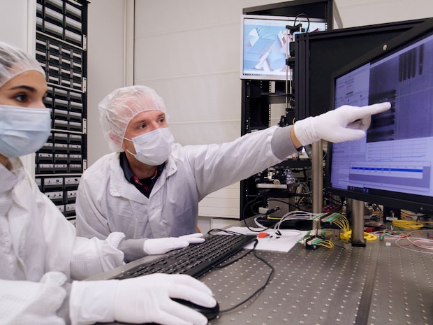
- Optical test and verification in lab: customized test rig
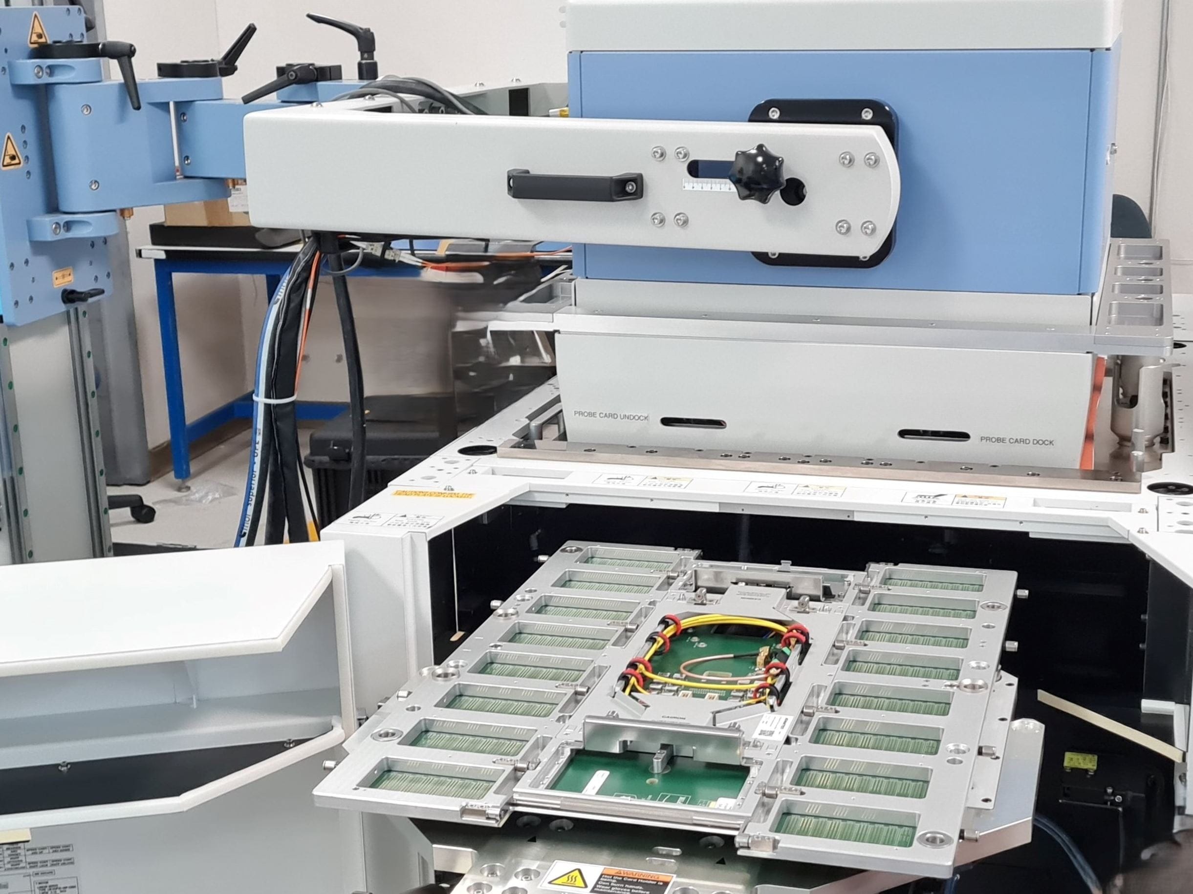
- Test under manufacturing conditions: Accretech UF3000 Prober

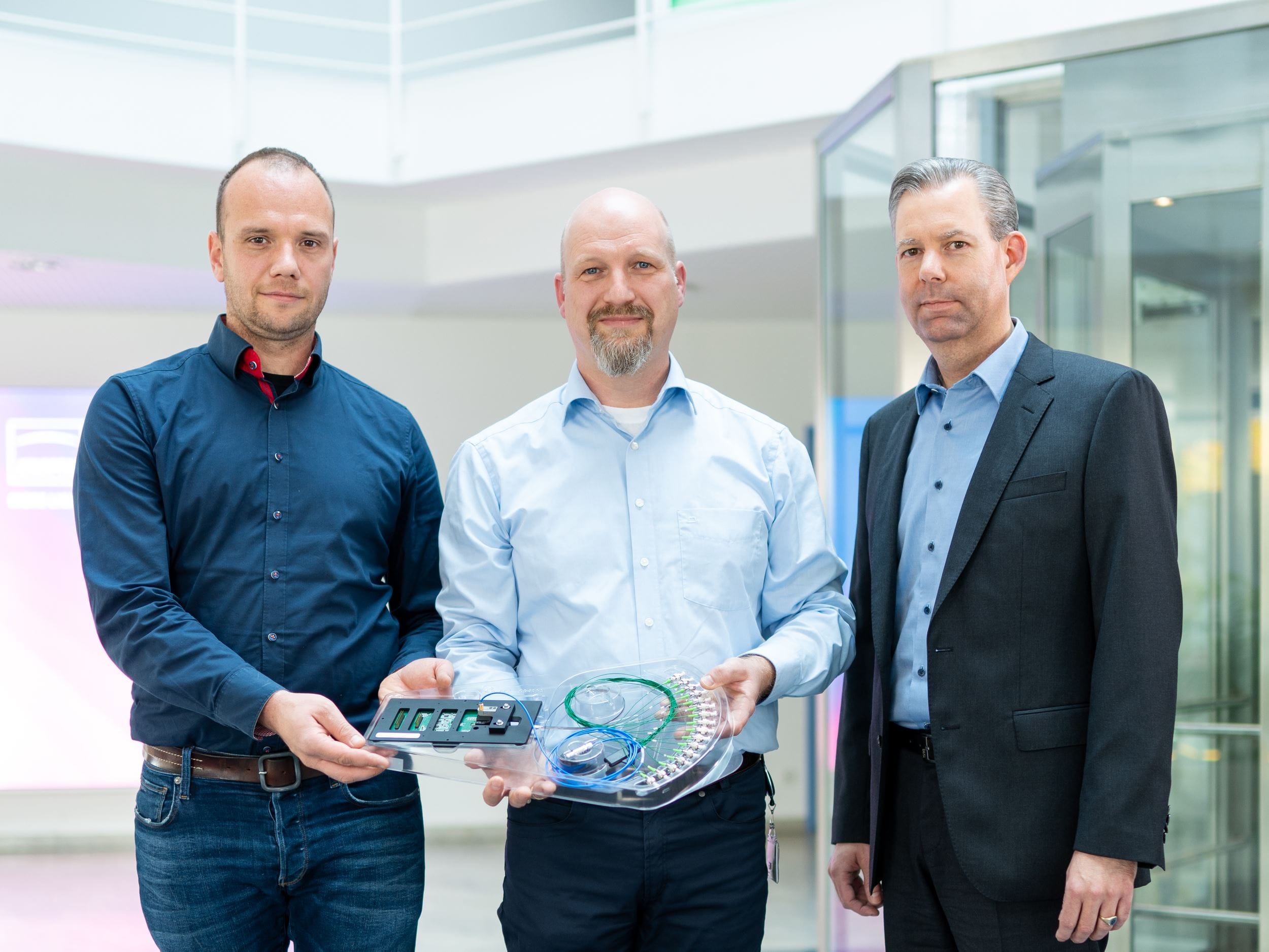
Awarded! Thuringia Innovation Award 2022 for UFO Probe® card
Jenoptik was awarded the Thuringia Innovation Award 2022 in the "Industry & Materials" category on November 30, 2022 in Weimar, Thuringia for its novel opto-electronic probe card for testing PIC wafers. Not quite 100 applications were received by STIFT Thüringen this year. Jenoptik convinced the expert jury with its well-thought-out approach to solving the increasing demand for photonic technologies in the electronics and semiconductor industry.